

Intel has made some design and manufacturing mistakes over the past few years, giving competitors such as AMD a certain advantage, and now the pioneer of x86 architecture is in the midst of an ambitious five-year plan to regain leadership in chipmaking, writes The Register.
The company is betting on Intel 4, a process formerly known as the manufacturer's 7-nm process technology. Intel plans to use it for products that will be released next year, including lithography for Meteor Lake processors for PCs and Granite Rapids server chips.
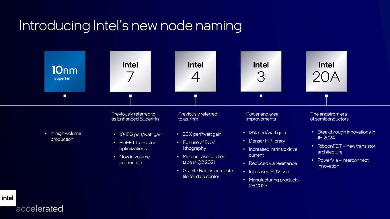
Earlier, Intel promised that Intel 4 would provide a 20% improvement in performance per watt compared to Intel 7, a process formerly known as 10-nm Enhanced SuperFin, which is used to make Alder Lake processors and recently deferred Sapphire Rapids server chips.
Ben Sell, chief executive officer of Intel 4, said the process was progressing well and that his team had achieved a 21.5% increase in performance for Intel 4 compared to Intel 7 at the same power. Conversely, Intel 4 can provide the same frequency level as Intel 7, using 40% less energy.
One of the achievements of Sell's Intel 4 bandwidth team is a 2-fold increase in capacitance of the metal-insulator-metal capacitor, which is the building block that Intel used for 14-nm process chips, which debuted in 2014 with the Broadwell processor.
Increasing the capacity leads to fewer large voltage fluctuations, which in turn increases the available voltage for the processor and allows it to run at higher frequencies.
Although increasing productivity is paramount to the new production process, it is also important to reduce costs and increase the reliability of chip production. In this regard, Sell says that his team has made significant progress through the use of Intel 4 lithography EUV, an advanced process that uses extreme ultraviolet light to etch the chip on silicon.
According to Sell, compared to the immersion process that Intel has used for previous nodes, EUV has allowed Intel to simplify the lithography process. In practice, this means Intel can reduce the number of layers required to etch chip designs onto silicon wafers from five to one.
"Everything now can be printed with a single layer to give you exactly the same structure," he said.
Using EUV also results in improved manufacturing yield, which means that the number of wafers with defects will go down. The other benefit of EUV is that it will lower Intel's chip-making costs for products using Intel 4, even though using EUV is expensive. However, it reduces the number of steps and the number of tools needed to make chips, according to Sell.
"There are many other tools outside of the lithography tools that we have in our factory and a lot of those are also not needed once you combine everything to a single step," says Ben Sell.
This simplified process could allow Intel to increase its production capacity, he said.
"That means you also get a lot less demand in terms of cleanroom space that you need. So overall, either you need to build fewer fabs, or you can get more output of each fab," explains Sell.
These and other process improvements are a more modular approach that Intel is taking before it develops new process technologies. This is a big change from the more aggressive approach that the chipmaker has previously used to develop process processes, which has led to serious errors and delays with 10-nm and 7-nm processes over the past few years.